side4linux, a simple integrated development environment!
PCBS Demo-2 Layout the Printed Circuit Board and create the Gerber files for the 'Try1' Project PCB.
Purpose: To
provide a basic introduction to creating a new Printed Circuit Board
design
using 'side4linux' 'gEDA' and 'pcb'. We will build a Serial
Communications input/output Printed Circuit Board from the schematic generated in Demo-1. Please keep in mind that
this is only a Demo, the actual printed circuit board of the Machine
Controller is to be presented in a later Demo along with exercises in how to use it so do not attempt to fabricate this board.
Requirements: Make sure that the 'GNOME' build environment is installed correctly, if not then read 'setup C build environment.txt' and also 'setup GNOME build environment.txt'.
Further requirements: Make sure that the latest PCBS
support package is installed correctly.
Pre-Requisites: Read through the Overview and do Demo-1 first.
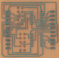
A photo of the bare PCB is shown next,
 Scanshot of the bare Serial1 PCB before the fitting of components. Note copper is on the component side.
So to begin making the PCB we will firstly look at the Sample2 examples,
- Open 'side4linux' and click on Project>Open Project in the Main Menue.
- Double click on the 'DEMOS' Product Area,
- Double click on the 'SIDEdemos' Product,
- In
the file dialog double click the 'PCBS' folder. This takes you
to where PCB projects are kept.
- Double click on 'Sample2', this opens the 'Sample2' project folder.
- Double click on 'Sample2.prf'. This opens the 'Sample2' project file.
- Notice
that the left bottom status bar window says 'Project: Sample2' which is the
Project Name.
- Notice that the next window says 'Ptype: PCBS' which is the
Project Type.
- Click
on the 'File Explorer' 'Files' tab on the left and view what schematic
files are actually in the Project ('serial1' &
'serial1_connectors').
- Click on 'Tools>PCBS>Run PCB, minimise the 'Component Library' window and maximise the main window of the 'pcb' program.
- Load the layout file 'serial1.new.pcb' from the main menue of 'pcb' ('File>Load Layout').
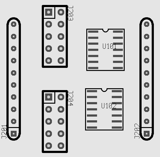
- It should look like the graphic below,
 Screenshot of the Sample2/Serial1 PCB Component Layout
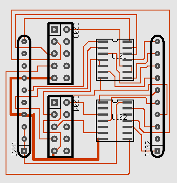
Now load the file 'serial1.pcb', this is the manually routed
printed circuit board. The earlier file is erased when you load a new
layout.

Screenshot of the Sample2/Serial1 PCB Manually Routed Layout, a 'single layer' board.
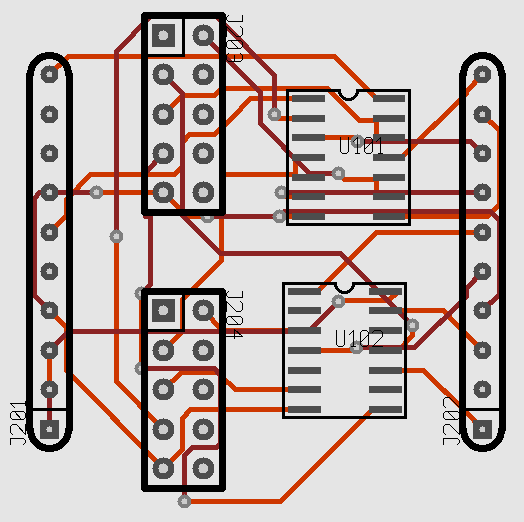
Now load the file 'serial1.autorouted.pcb', this is the automatically routed printed circuit board.

Screenshot of the Sample2/Serial1 PCB Auto Routed Layout.
- Pay attention to the 'square' index pins on the connectors, they are pin1.
- See if you can follow the schematic and compare that with the actual components and their 'track' connections.
- Notice the different track colours in the autorouted
example, red on the 'component side' (top) and brown on the 'solder
side' (bottom) of this 'two layer board'.
Practical 1: Run 'pcb' and load the Layout file for the 'Serial1' Printed Circuit Board,
Let us try to copy the 'Sample2' examples using Project 'Try1',
- Close the 'pcb' board program.
- Close the 'Sample2' Project 'Project>Close Project'.
- Open your Project 'Try1', Project>Open Project in the Main Menue of the IDE.
- Click
on the 'File Explorer' 'Files' tab on the left and view what schematic
files are actually in the Project ('serial1' &
'serial1_connectors').
- Click on 'Tools>PCBS>Run PCB, close the 'PCB Log ' window and maximise the main window of the 'pcb' program.
- Load the layout file 'board.pcb' from the main menue of 'pcb' ('File>Load Layout').
- Save the layout file as 'try1.pcb' 'File>Save layout as'.
- Remember that your are dealing with 'mils', A 'mil' is 1/1000th of an inch and spacing is usually in 10 mill increments.
- At this stage all you have is all the components bunched
up in the top left hand corner so try clicking on 'Select>Disperse
all elements'.
- Now drag and rotate the components to match the screen shot of the Sample2/Serial1 PCB Component Layout above.
- If you have forgotten how to drag and rotate then re-read the 'Overview'.
- Remember to save early and save often during your editing!
- Try to get all of the compenents within a 1.6 inch square (use the mouse cusor and read the X/Y values top right of screen).
- Now resize the board to 1.6 inches square.
-
Go to 'File>Preferences>Sizes>Board Size' and set both 'Width' and 'Height' to 1600.0 (1600 mils = 1.6 inches).
- At this point you can load the netlist file 'board.net' into the Layout, 'File>Load layout'.
- Close the 'PCB Netlist' window.
- Type a lower case 'o' that is 'ooh' and not zero!
- This should now expose the 'ratsnest' which is the unrouted connections of the board.
- Save the file again (keep doing this!).
- You should now have something like the following graphic on your screen,
 Screenshot of Try1's Layout with ratsnest.
Practical 2: Route the 'Serial1' Printed Circuit Board tracks and produce output files.
- At this point if you require a single layer board you
could manually route by selecting 'Line' mode and draw in the
tracks.
- We will make this short as it is only a Demo by using the
automatic routing facilities, click on 'Connects>Auto route all
tracks'.
- 'The PCB Log' window should come up with '30 of 30 nets
successfully routed. Congratulations!! The layout is complete and has
no shorted nets.'.
- Close the 'PCB Log' window and try using the autoroute optimisations 'Optimise autorouted tracks'.
- End with the 'Miter' optimisation.
- Save the Layout again (keep doing this!).
- Now for some output, 'File>Export layout>ps' to create a postscript print file of about ten pages.
- Now for the 'Gerber' and drill files for the board maker 'File"Export layout>gerber'.
- You could now save the layout file and close the 'pcb' program as we are now done with it.
- Close the Project and close down the side4linux IDE.
- In Practical-3 we will look at the output which could be used to make this demo board.
Practical 3: View the 'Serial1' Printed Circuit Board output files.
- You
may convert the postscript file from Demo-2 into 'PDF' using 'ps2pdf' (re-read the
Overview if you have forgotten).
- Open your 'PDF' reader and look at the pages of output, one of these could be used to create a 'master' using your printer.
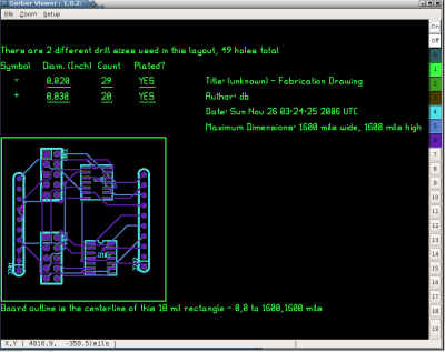
- Open the side4linux IDE and and the 'Try1' Project then select the gerber viewer 'Tools>PCBS>Gerber Viewer'.
- Click the 'On' button top right hand side.
- Try clicking layers on and off (coloured buttons' below 'On" button) to see what each layer is.
- View your work which should look something like the following graphic,
 Screenshot of the output of the Gerber viewer 'gerbv'
If this board was going to a commercial board maker ( and it is
only a demonstration exercise so it is not ) you would
send along the 'PDF' file that you have created along with the files
ending
in 'gbr' and the 'Excelon' 'cnc' drill file 'try1.plated hole.cnc'. The
'PDF' so the board maker can see what you want and the rest to
manufacture your board. Note that as this is a two sided board, you
need to specify to the board maker that you will require plated through
holes. Should you actually need a working example of the serial
interface then check out the Project 'Serial1' in the PCBS folder, this
is the
serial interface used with the prototype CPU shown in the 'overview'.
Please note that we will not be providing support for any prototype
Projects that we
are releasing so use prototypes at your own risk!

Screenshot of the real Serial1 PCB
(Note the header pins and the connector pins are on the same side to allow for a single sided board.
This means cutting an access hole in the 'mother board' to connect the headers to the serial outlet sockets!)
In Demo-3 we will build and assemble the Machine Controller programming interface PCB and cables.
We will provide other demos as 'side4linux' develops to
cover integration into a real world machine
controller.
