Practical 1: Open a schematic file in 'gEDA' the graphical schematic editor to view a schematic file graphically,
1/. Click on the 'Open-SCH' tool bar button and open the file 'cpu.sch'
This action will launch the schematic capture program 'gEDA' with the 'cpu.sch' schematic file as follows,
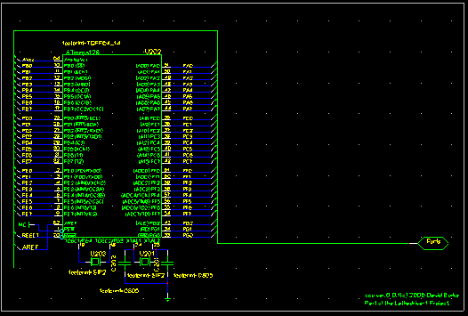
Screenshot of the CPU schematic in gEDA
This action will launch the schematic capture program 'gEDA' with the 'cpu.sch' schematic file as follows,

Screenshot of the CPU schematic in gEDA
- Keep in mind that this is only a copy of the file on disk, if you make changes then you must 'Save' them.
- Close the small 'Status' window and click on the top right hand "Maximize Window' button to make the window full size.
- Right click in the window to bring up the 'Popup Dialog' window and left click on 'Zoom Extents'.
- Move the mouse cursor to the center and while holding down the middle mouse button, drag the drawing a bit and let go.
- Place the mouse cursor over a crystal at the bottom ( U203 ) and zoom in/out by rolling the mouse wheel.
- Move the drawing using the window sliders on the right and bottom of the window.
- Notice that the pins of components are connected together by conducting wires called 'Nets' such as 'PE0' and 'RESET'.
- Notice that these 'Nets' are named and are kept neat by enclosing them in conduits/pipes called 'Buses'.
- Notice that the 'Bus' on this page is called 'Ports' ( the name is in the I/O 'off page connector at the right hand end).
- Notice the 'Net' 'AVcc' connected to pin 64 of the 'ATMega128' micro-controller chip ( U202 ).
- Keep in mind that 'Net Names' are 'Global' to the Project.
- So the Net on the 'cpu.sch' page called 'AVcc' is the same wire as Net 'AVcc' on the 'power.sch' page.
- Take note that 'Buses' and the off page connector have no electrical significance, it is just an information guide.
- Notice that each component has an ID code called a 'Reference Designator' or 'Ref-Des' such as U102 or C101.
- Reference designators must be unique.
- If you use the 'Renumber' Button on the IDE Toolbar they increment by 100 for each page in the Project e.g. page 3 start at 301.
- Notice the 'footprint' tags e.g. to the right of C201 is the footprint of '0805' which is an 0805 surface mount package (SMT).
- Footprints are the physical pads/holes used by the PCB program. Each schematic decal needs a physical footprint assigned to it.
- Notice the footprint for U202 is a TQFP64 which is a surface mounted Thin Quad Flat Package with 64 pads.
- Footprints can be found by opening the Symbol Library in the 'pcb' layout program.
You will notice the components are displayed graphically. They consist
mainly of the AVR Mega-128 decal and some support chips. Where is the
rest you may ask as this is just one page of many that we will use to
build this product. The paradigm is simple! You provide schematic
pages, each of a different function which together will make one
printed circuit board. You may well be wondering why we do not just put
everything on the one page, the answer is re-usability. By using this
'object' type approach one can build up a large library of schematic
pages which can be quickly assembled by adding them to the Project so
that it is possible to create many different Projects. One Project may
require the addition of 'RS232 Serial' ports, another 'Ethernet' and
even our Machine Controller will require different output driver boards
and interfaces to different position feedback sensors etc. etc. So take
another look in the 'Files' tab of the 'File Explorer' You will see
that this Project has only pages for power,
cpu (the one we are currently looking at) and a connector page for
three dual inline 20 pin male connectors. That is because this Project is a 'Daughter Board' that will eventually be plugged into a 'mother board'. From this introduction you
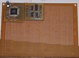
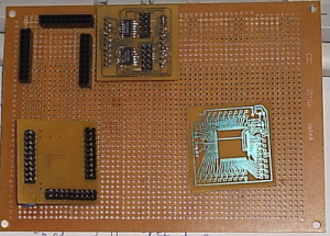
will see the completion of this CPU unit (pictures are included at the
end) as part of a larger Project, the 'Machine Controller'. Our aim is
to build the Machine Controller using plug in daughter boards onto a
larger 'mother board' and at a later date we will just leave out the
connector schematic pages and produce a single board Machine
Controller!
Practical 2: Open a 'Layout' file in 'pcb' the graphical PCB editor to do some editing,
Close down the 'gEDA' program and now click on 'TOOLS>PCBS>Run PCB' in the IDE to launch 'pcb' the PCB layout program. Once the 'pcb' layout program is loaded select a component 'footprint' in the smaller 'PCB library' window 'pcblib>~geda>TQFP64_14' by left clicking on it and move the cursor into the main pcb window to see the outline in red as shown in the following graphic,
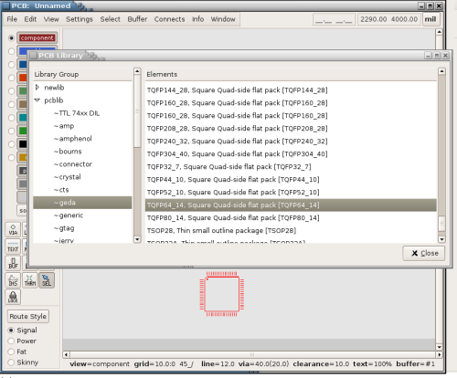
Screenshot of the 'pcb' component library with selected footprint in red.
This component footprint is a 'TQFP64' which is a surface mounted Thin Quad Flat Package with 64 pads. Notice the actual footprint name is at the end inside the square brackets as 'TQFP64_14'. When you assign footprints to a schematic page you must make sure that the correct footprint name is put into the schematic file (we will do this in Demo1) or the schematic to pcb program will not work properly as it will lock up endlessly looking for a non existent footprint!
Now press the escape key 'Esc' to release the library component footprint as we will not need it here then minmise the library window and maximise the main window of the 'pcb' program.
Take note that there are many parts to a printed circuit board! Some of them are,
Go to 'File>Preferences>Sizes>Board Size' and set both 'Width' and 'Height' to 1800.0 (1800 mils = 1.8 inches).
Now load the initial 'Layout' file . Click on 'File>Load Layout' in the 'pcb' program and open the original board layout file 'board.pcb'.
You can edit it to produce the following graphic, start with 'Select>Disperse all elements'.
Take note of,
Save this layout under the name of 'Try.pcb' 'File>Save layout as' and keep saving as you progress so as not to loose everything by mistake or system failure. To now continue you will need to manually pull the components apart by holding down the left mouse button and dragging them. You will also need to change 'editing state' from 'Selection' to 'Rotate' to rotate some components (click on 'ROT' in the 'Editing State' selector and left click on the component) to match the following view. When you have something like what is shown below click on 'File>Load netlist file' to load the connections netlist file 'board.net' which must be routed. Now press the 'o' letter on the keyboard to show the ratsnest that we will later show as routed tracks. (Notice that keyboard commands are 'case sensitive' therefore 'o' works but 'O' is a different command and a lot different from the zero key '0' !!!! Try manually routing a trace by clicking on the 'Component' button at the top of the 'Layer Selector' and changing the 'Editing State' to 'Draw Line' mode by clicking on 'LINE' in the 'Editing State' selector (you can return to 'Selection' by clicking on 'SEL'). Now start a line on one of the nets by left clicking with the mouse on the start point and left clicking at each corner. Once you have reached the other end press the escape key on the keyboard 'Esc'. The ratnest line under the routed line should now disappear when you reorganise the ratsnest by pressing the 'o' key. Remove your new trace by holding the mouse cursor over the trace segments one at a time and pressing the delete key on the keyboard 'Delete' or 'Del'. You could then try auto routing by clicking 'Connects>Auto route All nets'.
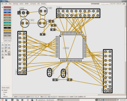
Screenshot of the CPU components with the ratsnest prior to routing.
Close the 'pcb' program and restart using 'TOOLS>PCBS>Run PCB' and now load the 'cpu.pcb' file and you should see the following,
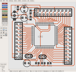
Screenshot of the CPU completed ready for the production of the 'Gerber' and 'drill' files that will go to your PCB maker.
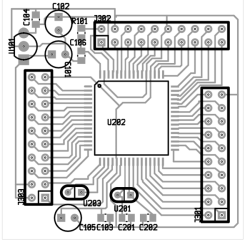
Screenshot of the Component Overlay (derived from the pcb print file)
Practical 3: Creating some output
Now that we have a PCB 'Layout' we need to view it as,
Practical 2: Open a 'Layout' file in 'pcb' the graphical PCB editor to do some editing,
Close down the 'gEDA' program and now click on 'TOOLS>PCBS>Run PCB' in the IDE to launch 'pcb' the PCB layout program. Once the 'pcb' layout program is loaded select a component 'footprint' in the smaller 'PCB library' window 'pcblib>~geda>TQFP64_14' by left clicking on it and move the cursor into the main pcb window to see the outline in red as shown in the following graphic,

Screenshot of the 'pcb' component library with selected footprint in red.
This component footprint is a 'TQFP64' which is a surface mounted Thin Quad Flat Package with 64 pads. Notice the actual footprint name is at the end inside the square brackets as 'TQFP64_14'. When you assign footprints to a schematic page you must make sure that the correct footprint name is put into the schematic file (we will do this in Demo1) or the schematic to pcb program will not work properly as it will lock up endlessly looking for a non existent footprint!
Now press the escape key 'Esc' to release the library component footprint as we will not need it here then minmise the library window and maximise the main window of the 'pcb' program.
Take note that there are many parts to a printed circuit board! Some of them are,
- Layout file (the actual layout of physical components such as chips, resistors, connectors etc.)
- Netlist file (the file containing the actual connections to pins, pads etc.)
- Pcb file ( the combination of the Layout and Netlist files that make up a PCB ).
- Output files (Gerber 'gbr' for the PCB maker, PS 'ps' postscript for your printer etc.)
- Annotation (altering the schematics in gEDA and forwarding the changes to your PCB drawing.)
- Drill files (the 'Excelon' format 'cnc' drill file used by your PCB maker to drill holes for IC's etc.)
- A 'ratsnest' is the unrouted connections from the 'netlist' file which you must load after the 'layout file'.
- Default values e.g. it is a good idea to set the board size prior to the initial load of the layout file!
Go to 'File>Preferences>Sizes>Board Size' and set both 'Width' and 'Height' to 1800.0 (1800 mils = 1.8 inches).
Now load the initial 'Layout' file . Click on 'File>Load Layout' in the 'pcb' program and open the original board layout file 'board.pcb'.
You can edit it to produce the following graphic, start with 'Select>Disperse all elements'.
Take note of,
- The 'Layer' selector (the rainbow coloured column in the top left corner).
- The 'Editing State' selector below it (changes 'Selection' to another state such as 'Rotate' or 'Line').
- The 'Route Style' selector in the bottom left corner (signal, power etc.).
Save this layout under the name of 'Try.pcb' 'File>Save layout as' and keep saving as you progress so as not to loose everything by mistake or system failure. To now continue you will need to manually pull the components apart by holding down the left mouse button and dragging them. You will also need to change 'editing state' from 'Selection' to 'Rotate' to rotate some components (click on 'ROT' in the 'Editing State' selector and left click on the component) to match the following view. When you have something like what is shown below click on 'File>Load netlist file' to load the connections netlist file 'board.net' which must be routed. Now press the 'o' letter on the keyboard to show the ratsnest that we will later show as routed tracks. (Notice that keyboard commands are 'case sensitive' therefore 'o' works but 'O' is a different command and a lot different from the zero key '0' !!!! Try manually routing a trace by clicking on the 'Component' button at the top of the 'Layer Selector' and changing the 'Editing State' to 'Draw Line' mode by clicking on 'LINE' in the 'Editing State' selector (you can return to 'Selection' by clicking on 'SEL'). Now start a line on one of the nets by left clicking with the mouse on the start point and left clicking at each corner. Once you have reached the other end press the escape key on the keyboard 'Esc'. The ratnest line under the routed line should now disappear when you reorganise the ratsnest by pressing the 'o' key. Remove your new trace by holding the mouse cursor over the trace segments one at a time and pressing the delete key on the keyboard 'Delete' or 'Del'. You could then try auto routing by clicking 'Connects>Auto route All nets'.

Screenshot of the CPU components with the ratsnest prior to routing.
Close the 'pcb' program and restart using 'TOOLS>PCBS>Run PCB' and now load the 'cpu.pcb' file and you should see the following,

Screenshot of the CPU completed ready for the production of the 'Gerber' and 'drill' files that will go to your PCB maker.

Screenshot of the Component Overlay (derived from the pcb print file)
Practical 3: Creating some output
Now that we have a PCB 'Layout' we need to view it as,
- Gerber 'gbr' files suitable to be sent to a board vendor of your choice or,
- As a Postscript file that can be printed as a mask for home manufacture or,
- As an isolation file that can be
milled in a CNC milling machine.
