side4linux, a simple integrated development environment!
PCBS Demo-1 Create a new PCBS Project based on 'Sample2' and complete the schematics..
Purpose: To
provide a basic introduction to creating a new Printed Circuit Board
design
using 'side4linux' 'gEDA' and 'pcb'. We will build a Serial
Communications input/output board to go with the demo CPU board which
together makes up our prototype Machine Controller. The new board will
be called 'Serial1' (that is shorthand for 'RS232C Serial interface
board number 1'). You
may of course not be interested in our Machine Controller. This is OK
as side4linux can build anything you wish! We simply ask
that you follow this Demo as an introduction on how to
use the IDE
and it's Tool set. Note also that you may have many invocations
of the side4linux IDE open so you may wish to use one to show this Help
while using another to do the Practicals. You could also print out this
page to have some hard copy available for reference (very good if you
are teaching a group of students as they may all have a photo copy). Please keep in mind that
this is only a Demo, the actual printed circuit board of the Machine
Controller is to be presented in a later Demo.
Requirements: Make sure that the 'GNOME' build environment is installed correctly, if not then read 'setup C build environment.txt' and also 'setup GNOME build environment.txt'.
Further requirements: Make sure that the latest PCBS
support package is installed correctly.
Pre-Requisites: Read through and understand the content in the Overview first.
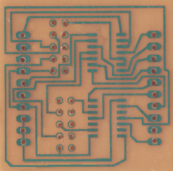
A photo of the PCB is shown next,

So to begin,
- Open 'side4linux' and click on 'Project>Open Project' in the Main Menue.
- Double click on the 'DEMOS' Product Area,
- Double click on the 'SIDEdemos' Product,
- In
the file dialog double click the 'PCBS' folder. This takes you
to where PCB projects are kept.
- Double click on 'Sample2', this opens the 'Sample2' project folder.
- Double click on 'sample2.prf'. This opens the 'Sample2' project file.
- Notice
that the left bottom status bar window says 'Project: Sample2' which is the
Project Name.
- Notice that the next window says 'Ptype: PCBS' which is the
Project Type.
- Try clicking on 'Project' on the Main Menue, you will notice that 'Close Project' is now active.
- Notice that project names are set to be an upper case
letter followed by lower case letters (easier on the IDE's Project routines).
- Click
on the 'File Explorer' 'Files' tab on the left and view what schematic
files are actually in the Project ('serial1' &
'serial1_connectors').
- Click on 'Open-SCH' in the Toolbar and open 'serial1.sch'.
- Close the smaller 'opening status' window and maximise the main window.
- Right click in the middle of the main window and left click on 'Zoom Extents' in the popup menue.
- Print the 'serial1' file to the printer 'File>Print', you will need this later on in the Demo.
- Close the 'serial1' schematic file by closing gEDA (left click on the 'X' in the top right hand corner.
- Close the 'Sample2' 'Project Project>Close Project' in the IDE.
Practical 1: Create a new PCBS Project,
Create a new Project called 'Try1' by following these steps,
- Click on 'Project>New Project.
- Left click on the 'combo box selector' and select 'PCB Project with PCB and Schematic files' as the Project Type.
- Left click on the 'Next' button.
- Select the 'SIDEdemos' Product Area and click 'Open'
- Select the 'product_directory' and click 'Open'
- Click on the Combo box selector, select 'SIDEdemos' and click on Next,
- In the 'Accept New Project' box enter the name of our new project as 'try1' (just try1 without the quote marks!).
- Left click on the 'Build' button.
- The bottom left 'Status' box should now say 'Project Try1' and the 'Status' box next to it should be 'Project Type: PCBS'
- Close the new Project, 'Project>Close Project'
- Reopen the new Project (done to read in Project specific information not available while creating it).
- Click on the 'Files' tab in the 'File Explorer' notebook (left hand side of the screen).
- Notice that there is only one schematic page called 'power' (this is created by default)
- We will not require this default page so remove it, left click on it to highlight it then 'Project>Remove File from Project'
- You will be asked in a dialog box if you really want to remove it, click on the 'OK' button.
- This brings up another dialog box but as we do not wish to rebuild the new Project yet click on the 'Cancel' button.
- Now we need two files the same as those in 'Sample2', if
you have forgotten them then open side4linux in another workspace for
reference.
- Click on 'File>New File' and select 'New Schematic File'.
- In the dialog box remove 'Untitled' and put in 'Serial1' without the quote marks and click the 'OK' button.
- Click on 'Open-SCH' on the Toolbar of the IDE and have a look at the new blank file 'Serial1'.
- In the bottom right hand corner is the title as 'Serial1 ver.0.0.1(c) 2006 ?? Part of the Try1 Project.'
- Close gEDA and add the new schematic file to the Project, 'Project>Add File to Project'.
- In the dialog box that opens left click on 'Serial1.sch' to highlight it then click on the 'Add' button
- This time click the 'OK' button to rebuild the Project.
- Check that 'Serial1' now appears in the 'Files' tab of the File Explorer and close the Project.
- Open 'nautilus' and copy the file 'Serial1_connectors.sch' to the 'src' directory of the 'Try1' Project.
- Reopen the 'Try1' Project and add the 'Serial1_connectors.sch' file to the Project and accept rebuild of the Project.
- At this point click on the 'Files' tab in the 'File Explorer' and view the two pages in the Project.
- Place the mouse cursor on 'Serial1_connectors' in the File Explorer and while holding down the left mouse button drag the page below 'Serial1'.
- This puts the files in the right order with 'Serial1' first so components will start at 101 on this page and 201 on the next.
- Now rebuild the Project, 'Project>Rebuild Project from Tree.
- Try opening each file one at a time with 'Open-SCH' to ensure all is well.
- Close the Project.
- Close the IDE.
Practical 2: Place components into the 'Serial1' schematic,
In this Practical we will add
the components and the wires/buses needed to match the printout of
'Serial1.sch' that we printed earlier from the 'Sample2' Project. Make
note here that you can open this project in another copy of side4linux
at any time, preferably in another workspace but do try not to alter
'Sample2' by mistake! The Serial1 board that we are making will provide
the CPU with an RS232C serial communications interface, one output port
(DTE) and one input port (DCE) if you are not sure about RS232C then
look HERE.
- Open the 'Try1' Project in a fresh invocation of the side4linux IDE and click on 'Open-SCH' in the Toolbar of the IDE.
- Open the page 'serial1.sch' in gEDA, close the 'Opening Status' window, maximise the main window and zoom extents .
- We are going to add two components an MC1488 serial bus line driver and an MC1489 serial bus line receiver.
- Click on 'Add Component' on the gEDA Taskbar (looks like a two input logic AND gate!).
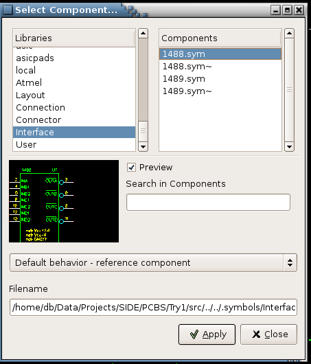
- In the left hand column of the 'Select Component' dialog
highlight 'Interface' with a left click and then in the right hand box
'1488.sym'
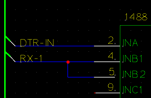
- Click on 'Apply' and moving the green component decal about where it is on your 'Sample2' printout left click once to place the component.
- Now press the escape key to disengage the selection (you
could left click to place more before clicking escape but one will do!).
- Place the mouse cursor over the component and left click once to turn it red (selected).
- Now once selected hold down the left mouse button over the decal and drag it to the correct spot.
- Left click in clear space on the main window to turn the decal back to green (de-selected).
- Do the same to place a MC1489 component into the schematic page as in your 'Sample2' printout.
- Notice that the component ID is U?? We will 'renumber' the components later.
- Now close gEDA, close the Project and close the IDE. It is time for my caffeine break!

Selection of Component from gEDA component library.
Practical 3: 'Wire up' the components in the 'Serial1' schematic,
In this Practical we will add connections to
the component 'pins' with 'nets' (also known as 'wires' or just 'connections') .
- Open the 'Try1' Project in a fresh invocation of the side4linux IDE and click on 'Open-SCH' in the Toolbar of the IDE.
- Open the page 'serial1.sch' in gEDA, close the 'Opening Status' window, maximise the main window and zoom extents .
- Add the buses shown by firstly left clicking on 'Add Buses mode' on the gEDA Toolbar.
- Use your printout as a guide (the buses are the thick lines).
- Note that buses and off page connectors have no electrical significance, they are just a visual guide!
- Buses are really just piping or conduit which keeps wiring layouts neat.
- Buses are added by left clicking at the start and right clicking at the end while in 'Add Buses' mode.
- After you have laid out your buses click on 'Select mode' on the gEDA Toolbar and add the Off page Connector 'intepage_bidir'.
- To do this click on 'Add component' on the Taskbar and
select from the 'Connection' parts library, place with left click then
right click.
- Place mouse over the new part and type 'er' in lower case to rotate then hold down the left mouse button and drag into place.
- Left click on the new component to select it (colour green
goes to red) and then double left click to bring up the 'Properties'
editor.
- Left click on 'pages' and then right click, select
'delete' by a left click. This will remove the 'pages' property from
the main window.
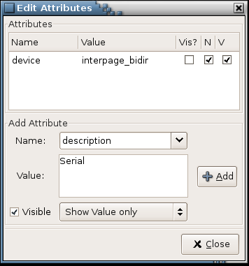
- Now add the name to the connector by clicking on the down arrow of the combo box and selecting 'description'.
- Type 'Serial' into the 'value' box, set up for 'Show Value Only' and click the 'Add' button as seen below,
Practical 4: Add 'footprints' to the components in the 'Serial1' schematic,
In this Practical we will add
the component footprint that the pcb program 'pcb' will need for your new board's pads or pin holes.
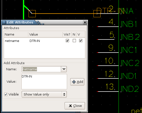
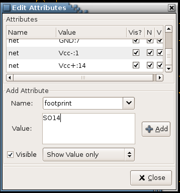
- Highlight the MC1488 component in 'Select mode ' (red) and double click on it to bring up the 'Edit Attributes' dialog box.
- Now add a footprint by clicking on the 'Name' combo box
down arrow and selecting 'footprint', type in the Value 'SO14' (small
outline 14 pad surface mount).
- Do the same for the MC1489 component as well, selecting and dragging the footprints into place as per your original printout.
- Bring
up the other schematic page in the Project and see how the 'netnames'
have at least one beginning at a pin in one sheet and an end either on
this sheet or the other sheet.
- Obviously all pins of the components must be connected
either to a 'net' or to the special 'net' of 'NC' (not connected
symbol) see pin 62 AREF on cpu.sch, Sample1.
- Expect DRC errors if there are interconnected nets (short circuits) or non-connected nets (open circuits).
- That completes the schematic requirements for this serial
interface board so in the next practical we will begin to produce the
pcb.

Adding a Footprint to a Component
Practical 5: Prepare the Netlist and Layout files for the 'Serial1' Printed Circuit Board,
In this Practical we will
renumber the components in the Project, run the DRC (schematic design rules
check) and convert the gEDA's schematic file into the 'pcb' program's 'netlist' and
'layout' files. Refer to the 'Overview' if you get lost at some point in these Exercises!
- Close gEDA if still open and and ensure that the 'serial1'
page is above the 'serial1_connectors' page in the 'Files' tab of the
File Explorer.
- Click on the 'Renumber' Toolbar button in the IDE and observe the output in the IDE's Output window.
- It should read that it has processed both pages without
error (you can open another IDE and run 'Sample2' in parallel for a
comparison).
- Click on 'DRC' and check the output, there should be no errors or warnings found.
- Click on 'Sch->PCB' to make the conversion. An 'Xterm'
window will open and should close by itself before five minutes is up,
if not then close it yourself.
- If there are errors they are likely to be footprint errors so check the printout of your schematics against those of 'Sample2'.
- Once successful you can close the Project and the IDE as it is the end of Demo-1!
In Demo-2 we will Layout the Printed Circuit Board and create the Gerber files for the 'Try1' Project PCB.
We will provide other demos as 'side4linux' develops to
cover integration into a real world machine
controller.
